- 您现在的位置:买卖IC网 > Sheet目录3818 > PIC18F4620-I/ML (Microchip Technology)IC MCU FLASH 32KX16 44QFN
PIC17C4X
DS30412C-page 76
1996 Microchip Technology Inc.
12.1.3.1
PWM PERIODS
The period of the PWM1 output is determined by
Timer1 and its period register (PR1). The period of the
PWM2 output can be software congured to use either
Timer1 or Timer2 as the time-base. When TM2PW2 bit
(PW2DCL<5>) is clear, the time-base is determined by
TMR1 and PR1. When TM2PW2 is set, the time-base
is determined by Timer2 and PR2.
Running two different PWM outputs on two different
timers allows different PWM periods. Running both
PWMs from Timer1 allows the best use of resources by
freeing Timer2 to operate as an 8-bit timer. Timer1 and
Timer2 can not be used as a 16-bit timer if either PWM
is being used.
The PWM periods can be calculated as follows:
period of PWM1 =[(PR1) + 1] x 4TOSC
period of PWM2 =[(PR1) + 1] x 4TOSC or
[(PR2) + 1] x 4TOSC
The duty cycle of PWMx is determined by the 10-bit
value DCx<9:0>. The upper 8-bits are from register
PWxDCH and the lower 2-bits are from PWxDCL<7:6>
(PWxDCH:PWxDCL<7:6>).
shows
the
maximum PWM frequency (FPWM) given the value in
the period register.
The number of bits of resolution that the PWM can
achieve depends on the operation frequency of the
device as well as the PWM frequency (FPWM).
Maximum PWM resolution (bits) for a given PWM fre-
quency:
The PWMx duty cycle is as follows:
PWMx Duty Cycle =
(DCx) x TOSC
where
DCx
represents
the
10-bit
value
from
PWxDCH:PWxDCL.
If DCx = 0, then the duty cycle is zero. If PRx =
PWxDCH, then the PWM output will be low for one to
four
Q-clock
(depending
on
the
state
of
the
PWxDCL<7:6> bits). For a Duty Cycle to be 100%, the
PWxDCH value must be greater then the PRx value.
The duty cycle registers for both PWM outputs are dou-
ble buffered. When the user writes to these registers,
they are stored in master latches. When TMR1 (or
TMR2) overows and a new PWM period begins, the
master latch values are transferred to the slave latches
and the PWMx pin is forced high.
Note:
For PW1DCH, PW1DCL, PW2DCH and
PW2DCL registers, a write operation
writes to the "master latches" while a read
operation reads the "slave latches". As a
result, the user may not read back what
was just written to the duty cycle registers.
log
(
FPWM
log (2)
FOSC
)
bits
=
The user should also avoid any "read-modify-write"
operations on the duty cycle registers, such as: ADDWF
PW1DCH
. This may cause duty cycle outputs that are
unpredictable.
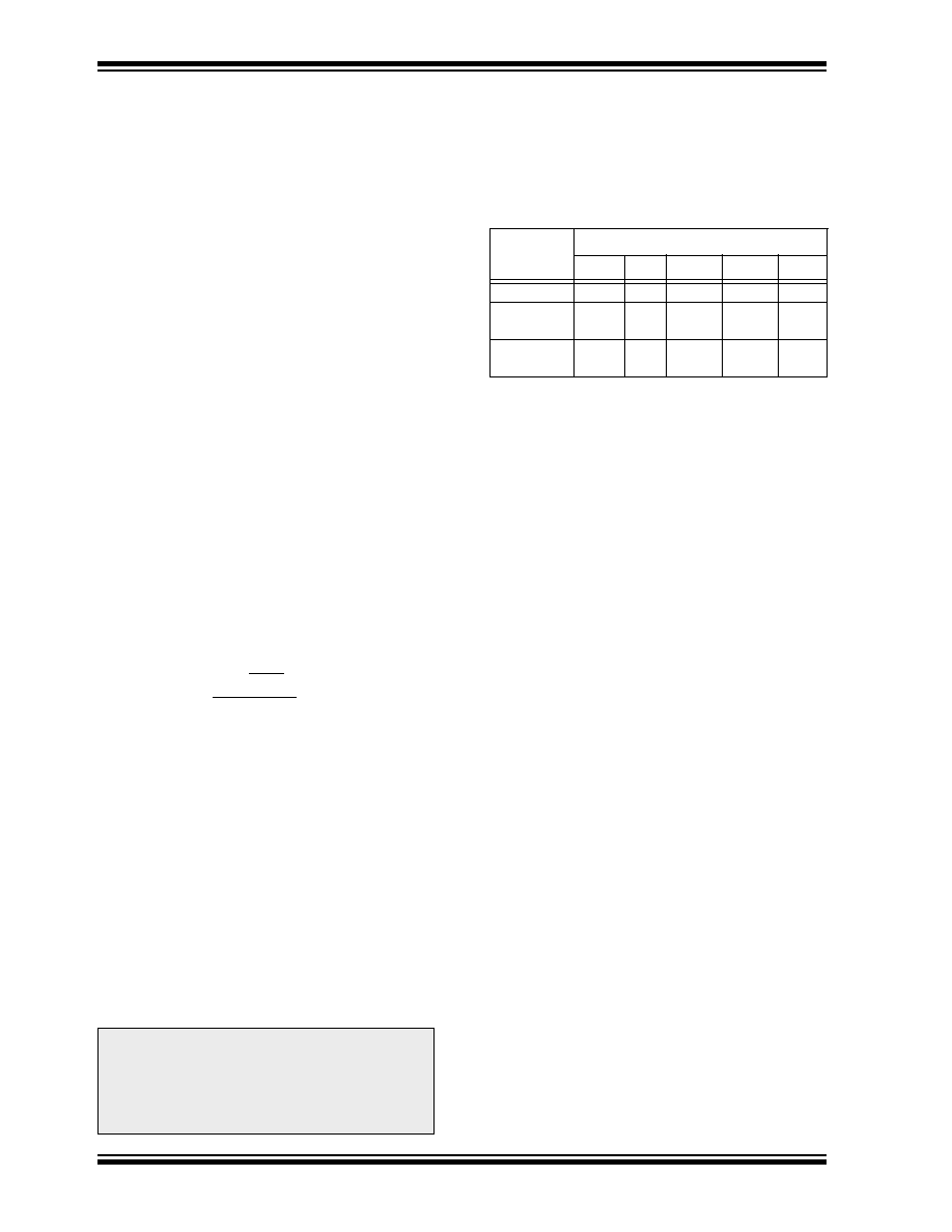
TABLE 12-3:
PWM FREQUENCY vs.
RESOLUTION AT 25 MHz
12.1.3.2
PWM INTERRUPTS
The PWM module makes use of TMR1 or TMR2 inter-
rupts. A timer interrupt is generated when TMR1 or
TMR2 equals its period register and is cleared to zero.
This interrupt also marks the beginning of a PWM
cycle. The user can write new duty cycle values before
the timer roll-over. The TMR1 interrupt is latched into
the TMR1IF bit and the TMR2 interrupt is latched into
the TMR2IF bit. These ags must be cleared in soft-
ware.
12.1.3.3
EXTERNAL CLOCK SOURCE
The PWMs will operate regardless of the clock source
of the timer. The use of an external clock has ramica-
tions that must be understood. Because the external
TCLK12 input is synchronized internally (sampled once
per instruction cycle), the time TCLK12 changes to the
time the timer increments will vary by as much as TCY
(one instruction cycle). This will cause jitter in the duty
cycle as well as the period of the PWM output.
This jitter will be
±TCY, unless the external clock is syn-
chronized with the processor clock. Use of one of the
PWM outputs as the clock source to the TCLKx input,
will supply a synchronized clock.
In general, when using an external clock source for
PWM, its frequency should be much less than the
device frequency (Fosc).
PWM
Frequency
Frequency (kHz)
24.4
48.8
65.104
97.66
390.6
PRx Value
0xFF
0x7F 0x5F
0x3F
0x0F
High
Resolution
10-bit
9-bit
8.5-bit
8-bit
6-bit
Standard
Resolution
8-bit
7-bit
6.5-bit
6-bit
4-bit
发布紧急采购,3分钟左右您将得到回复。
相关PDF资料
PIC24HJ256GP210-I/PT
IC PIC MCU FLASH 128KX16 100TQFP
PIC24HJ128GP310A-I/PF
IC PIC MCU FLASH 128KB 100-TQFP
DSPIC33FJ128GP310-I/PF
IC DSPIC MCU/DSP 128K 100TQFP
PIC16C66-20I/SO
IC MCU OTP 8KX14 PWM 28SOIC
DSPIC33FJ128MC510-I/PT
IC DSPIC MCU/DSP 128K 100TQFP
PIC16C66-20I/SP
IC MCU OTP 8KX14 PWM 28DIP
PIC18LF2620-I/SP
IC MCU FLASH 32KX16 28SDIP
PIC16F877-04I/P
IC MCU FLASH 8KX14 EE 40DIP
相关代理商/技术参数
PIC18F4620-I/P
功能描述:8位微控制器 -MCU 64KB 3968 RAM 36 I/O RoHS:否 制造商:Silicon Labs 核心:8051 处理器系列:C8051F39x 数据总线宽度:8 bit 最大时钟频率:50 MHz 程序存储器大小:16 KB 数据 RAM 大小:1 KB 片上 ADC:Yes 工作电源电压:1.8 V to 3.6 V 工作温度范围:- 40 C to + 105 C 封装 / 箱体:QFN-20 安装风格:SMD/SMT
PIC18F4620-I/P
制造商:Microchip Technology Inc 功能描述:IC 8BIT FLASH MCU 18F4620 DIP40
PIC18F4620-I/PT
功能描述:8位微控制器 -MCU 64KB 3968 RAM 36 I/O RoHS:否 制造商:Silicon Labs 核心:8051 处理器系列:C8051F39x 数据总线宽度:8 bit 最大时钟频率:50 MHz 程序存储器大小:16 KB 数据 RAM 大小:1 KB 片上 ADC:Yes 工作电源电压:1.8 V to 3.6 V 工作温度范围:- 40 C to + 105 C 封装 / 箱体:QFN-20 安装风格:SMD/SMT
PIC18F4620-I/PT
制造商:Microchip Technology Inc 功能描述:IC 8BIT FLASH MCU 18F4620 TQFP44
PIC18F4620T-I/ML
功能描述:8位微控制器 -MCU 64KB 3968 RAM 36 I/O RoHS:否 制造商:Silicon Labs 核心:8051 处理器系列:C8051F39x 数据总线宽度:8 bit 最大时钟频率:50 MHz 程序存储器大小:16 KB 数据 RAM 大小:1 KB 片上 ADC:Yes 工作电源电压:1.8 V to 3.6 V 工作温度范围:- 40 C to + 105 C 封装 / 箱体:QFN-20 安装风格:SMD/SMT
PIC18F4620T-I/PT
功能描述:8位微控制器 -MCU 64KB 3968 RAM 36 I/O RoHS:否 制造商:Silicon Labs 核心:8051 处理器系列:C8051F39x 数据总线宽度:8 bit 最大时钟频率:50 MHz 程序存储器大小:16 KB 数据 RAM 大小:1 KB 片上 ADC:Yes 工作电源电压:1.8 V to 3.6 V 工作温度范围:- 40 C to + 105 C 封装 / 箱体:QFN-20 安装风格:SMD/SMT
PIC18F4680-E/ML
功能描述:8位微控制器 -MCU 64KB 3328 RAM w/ECAN RoHS:否 制造商:Silicon Labs 核心:8051 处理器系列:C8051F39x 数据总线宽度:8 bit 最大时钟频率:50 MHz 程序存储器大小:16 KB 数据 RAM 大小:1 KB 片上 ADC:Yes 工作电源电压:1.8 V to 3.6 V 工作温度范围:- 40 C to + 105 C 封装 / 箱体:QFN-20 安装风格:SMD/SMT
PIC18F4680-E/P
功能描述:8位微控制器 -MCU 64KB 3328 RAM w/ECAN RoHS:否 制造商:Silicon Labs 核心:8051 处理器系列:C8051F39x 数据总线宽度:8 bit 最大时钟频率:50 MHz 程序存储器大小:16 KB 数据 RAM 大小:1 KB 片上 ADC:Yes 工作电源电压:1.8 V to 3.6 V 工作温度范围:- 40 C to + 105 C 封装 / 箱体:QFN-20 安装风格:SMD/SMT